Templated Crystallization in Metal-Halide Perovskite Optoelectronics
Crystals invariably grow from a medium, which influences their formation. Templated crystallization
uses an external template, like a surface or molecule, to guide the formation of crystals,
influencing their shape, size, composition, and even the type of crystal that forms (i.e. polymorphism).
A classic case is the biogenic crystallization of guanine in zebrafish. The morphology and composition
of guanine crystals vary by tissue: in the skin, they form square or hexagonal platelets that assemble
into organized stacks, producing iridescent coloration; in the eye, they adopt elongated shapes and
arrange into multilayer arrays to enhance light reflection for improved vision in low-light conditions.
The morphogenesis of guanine crystals is "templated" by genetic factors (Fig. 1).
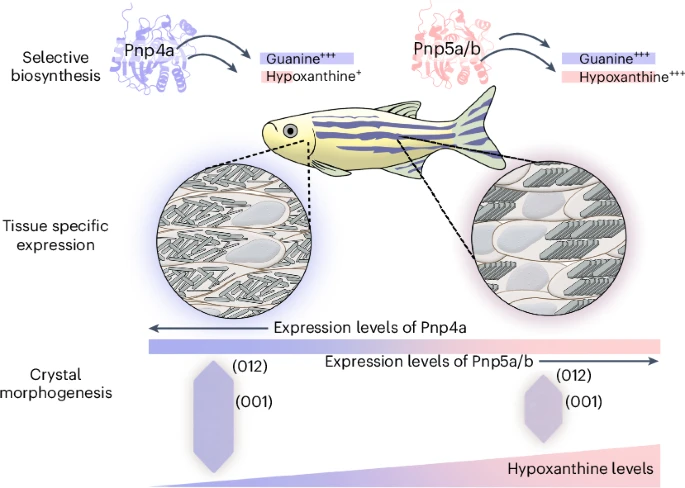
Fig 1. Genetic control over biogenic crystal morphogenesis in zebrafish [1]
Inspired by biology, materials scientists have explored templated crystallization of synthetic
nanomaterials since the late 20th century. In recent years, interest has shifted toward metal-halide
perovskites and the use of organic molecules as "molecular templates." Metal-halide perovskites are
a class of ionic semiconductors that adopt the classic "ABX3" perovskite structure (Fig. 2a), where B is a
divalent metal cation (Pb2+ or Sn2+), X represents halides (Cl-, Br-,
or I-), and A typically consists of small monovalent cations, such as organic methylammonium
(MA+) and formamidinium (FA+), or inorganic Cs+. Their soft ionic lattice
enables solution processing at mild conditions, while compositional tunability allows for bandgap control
from visible to near-infrared, making them interesting light absorbers and emitters. With low-cost
fabrication and tunable properties, metal-halide perovskites has become promising alternatives to
silicon in solar cells, while interest also extends to solid-state lighting, photodetectors,
quantum materials, and photonic integration.
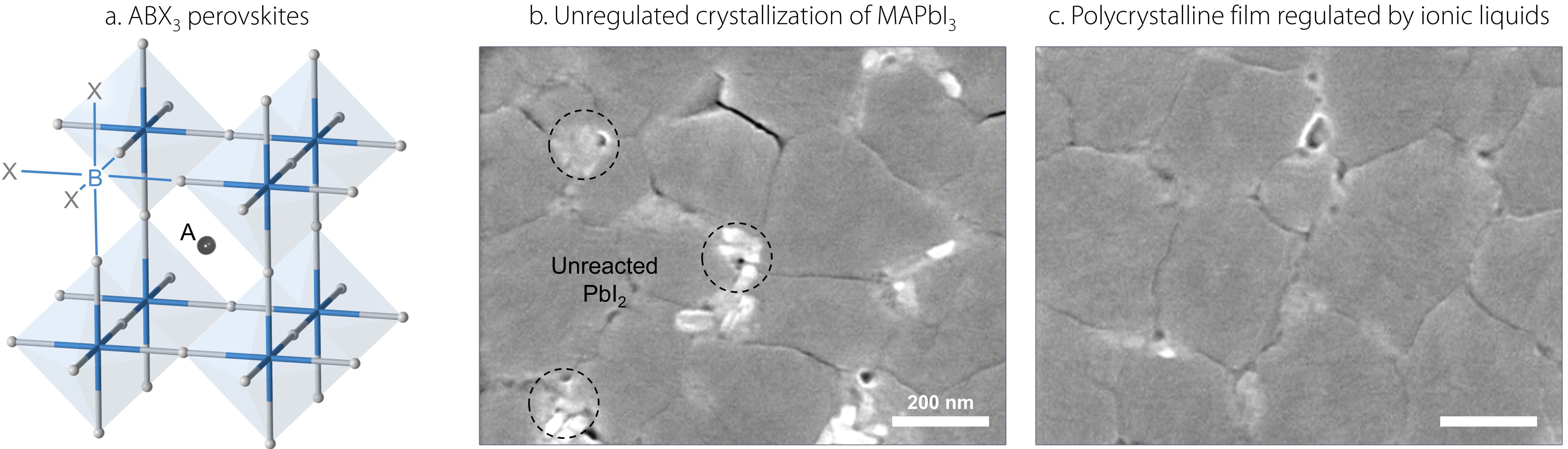
Fig 2. (a) The structure of classic ABX3 perovskites. (b,c) Perovskite polycrystalline
film morphology (b) without and (c) with ionic liquid additive. Images from scanning electron microscopy (SEM). [2]
Compositional and morphological control are critical in semiconductor devices. In metal-halide perovskites,
compositional control primarily involves minimizing defects and impurities. While perovskites are more
defect-tolerant than silicon, which requires ultra-high purity over 99.9999999% (9N), their compositional
complexity and solution processing introduce challenges. For example, unreacted PbI2 is a major
issue in MAPbI3, a widely used low-bandgap perovskite for solar cells, as rapid crystallization
often prevents complete precursor conversion (Fig. 2b). PbI2, now as an impurity, is known to decompose
into gaseous I2 and metallic Pb(0) under light and thermal stress during solar cell operation,
acting as catalytic sites that accelerate perovskite degradation and compromise device stability.
Alternatively, crystallization can be regulated by capturing PbI2 precursors and gradually
converting them to MAPbI3. We recently developed an ionic liquid as a molecular template
for this purpose. Ionic liquid is a type of organic salt with low melting point and usually behave as
liquid near room temperature, which makes them compatible with the processing of ionic metal-halide
perovskites. Our designed ionic liquid strongly coordinates with PbI2, forming an adduct
that mediates crystallization and enables near-complete precursor conversion. This controlled process
reduces PbI2 aggregates, increases perovskite grain size, and yields smooth, low-defect
polycrystalline films (Fig. 2c).
Morphological control in optoelectronic devices extends beyond individual crystals to the spatial
organization of grains in polycrystalline thin films. While in solar-cells, grains need to be closely
connected and grain boundaries carefully managed to ensure efficient extraction of photogenerated charge
carriers, this may not be the case in light emitting diodes (LEDs), where injected charges generate photon,
or light, as output. Metal-halide perovskites, as excellent direct-bandgap semiconductors, can achieve
near-unity internal quantum efficiency (IQE), meaning nearly all injected electrons generate photons.
Nonetheless, external quantum efficiency (EQE), which concerns the photons actually emitted, can remain
low due to poor outcoupling efficiency (OCE), where a significant portion of generated light is trapped
within the device rather than emitted from the display area.
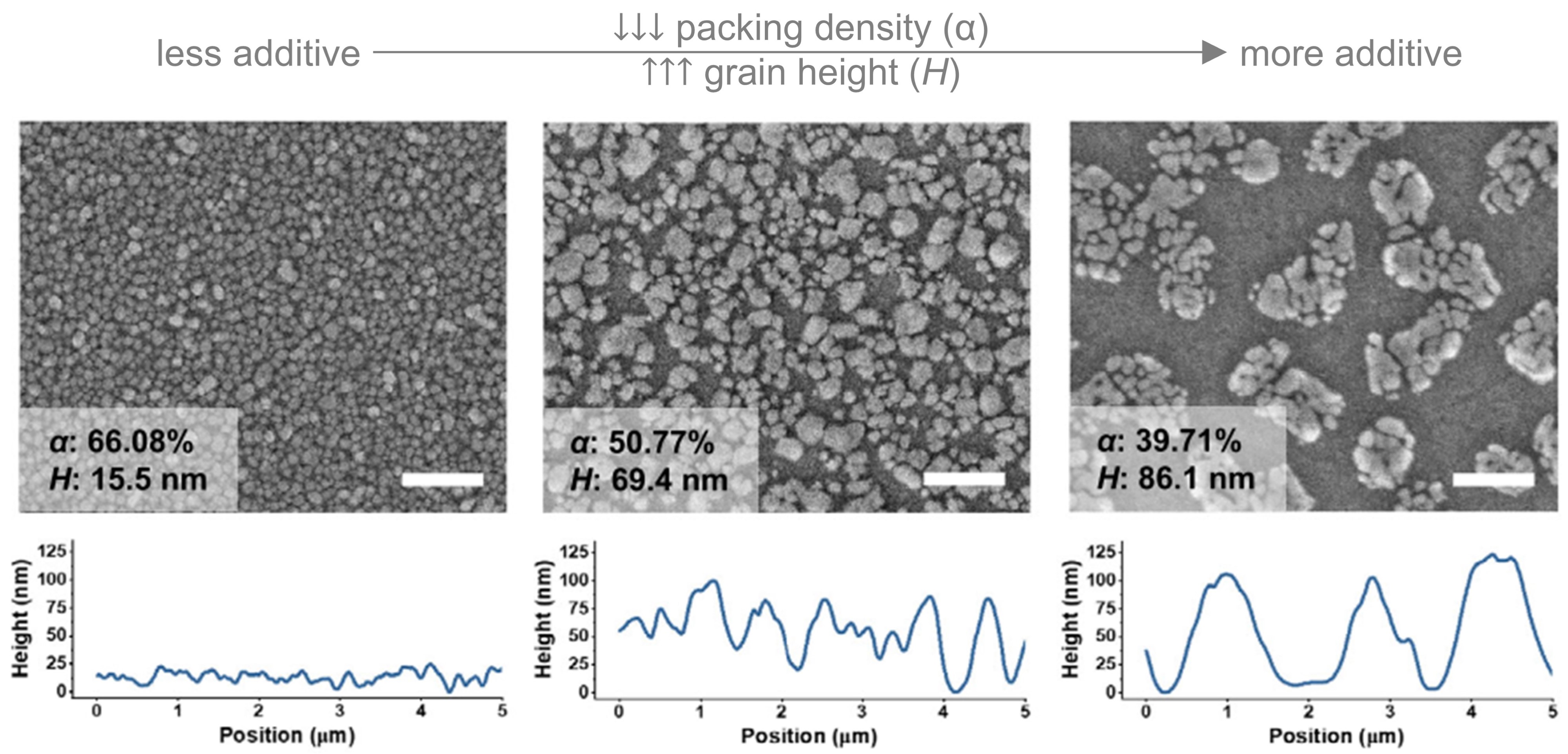
Fig 3. SEM images of perovskite films with segregated grains gradually amplified
with increasing additives (scale bar: 1 μm). Bottom: height profile from atomic force microscopy. [3]
Low OCE is a common challenge in continuous polycrystalline films, as light is easily waveguided to the
device edges. A smart solution to this is the formation of segregated instead of continuous grains. The
in-situ bottom-up formation of polycrystalline perovskite films can be templated by a combination of
substrate effects, additives, and solvents. Surprisingly, the careful control of these factors gave rise
to the spontaneous formation of discrete islands of perovskite crystals with controllable size and packing
density (Fig. 3). Randomly distributed perovskite crystals act as discrete emitters and scatterers, which when
combined with sequentially deposited layers, form convex structures. Due to the high reflectivity of
electrodes, these convex domes effectively function as microlenses to facilitate the extraction of light
that would otherwise be confined in waveguide modes. This unique "discrete island–convex dome" morphology
resulted in dramatically increased OCE, and thus highly efficient perovskite LEDs (Fig. 4).
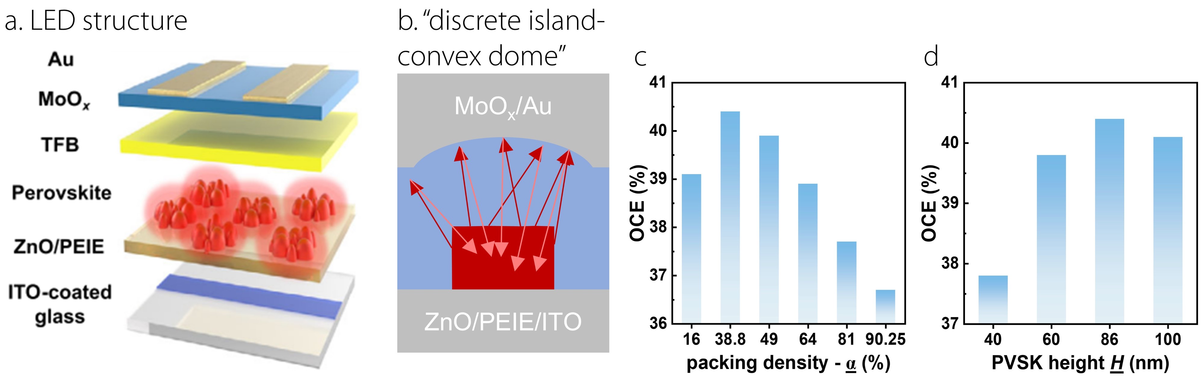
Fig 4. (a) Device structure of a perovskite LED. ZnO/PEIE is the carrier (hole) transporting
layer as well as the substrate templating isolated grain formation when perovskites are deposited. (c) A scheme of the
"discrete island - convex dome" structure with light emitted from perovskites been efficiently reflected and concentrated.
(c,d) Simulated OCE with varying packing density and grain height. [3]
In summary, crystallization is a holistic process that discusses both internal and external factors.
Modern semiconductors come with considerable compositional complexity yet also brings exciting
opportunities for templated crystallization. The concept of "molecular templating" raised here in
metal-halide perovskites illustrates how complex control in optoelectronic devices can converge to
simple molecular reasons, and hence highlighting the hierarchical aspect of our molecular design.
Note: the writing here conveys a perspective of the field
Read more:
[1]
Genetic control over biogenic crystal morphogenesis in zebrafish.
Nat. Chem. Biol. 2025, 21, 383-392.
[2] Xu, W.+; Shao, W.+; Tang, Y.; Lin, C.; Yang, H.; Yang, Y. -T.; Kim, J. H.; Lee, G.;
Kumar, P.; Pedersen, K. R.; Coffey, A. H.; Harvey, S. P.; Graham, K. R.; Zhu, C.; Zhu, K.; Dou, L.
Ionic Liquids Improve Perovskite Solar Cells Long-Term Stability.
Submitted.
[3] Baek, S. -B.+; Shao, W.+; Feng, W. -J.; Tang, Y.; Lee, Y. H.; Loy, J.; Gunnarsson, W. B.;
Yang, H.; Zhang, Y.; Faheem, M. B.; Kaswekar, P. I.; Atapattu, H. R.; Coffey, A.; Park, J. Y.; Yang, S. J.; Yang, Y. -T.;
Zhu, C.; Wang, K.; Graham, K.; Gao, F.; Qiao, Q.; Guo, L. J.; Rand, B.; Dou, L.
Grain Engineering for Efficient Near-Infrared Perovskite Light-Emitting Diodes.
Nat. Commun. 2024, 15, 10760.